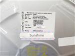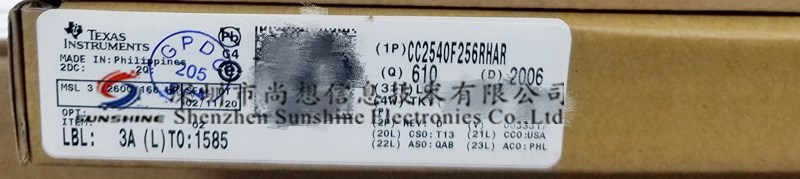
CC2540F256RHAR
TI
QFN40
20+
企业名:深圳市尚想信息技术有限公司
类型:贸易/代理/分销
电话:
0755-83948880
0755-8398880
手机:15323892334
18182115682
联系人:姚小姐/邓小姐
QQ: 
微信:
邮箱:assistant@sunshineic.com
地址:广东深圳福田区振兴路上步工业区405栋6楼603室
The 8051 CPU core is a single-cycle 8051-compatible core. It has three different memory access busses (SFR,
DATA, and CODE/XDATA), a debug interface, and an 18-input extended interrupt unit.
The memory arbiter is at the heart of the system, as it connects the CPU and DMA controller with the physical
memories and all peripherals through the SFR bus. The memory arbiter has four memory-access points, access
of which can map to one of three physical memories: an SRAM, flash memory, and XREG/SFR registers. It is
responsible for performing arbitration and sequencing between simultaneous memory accesses to the same
physical memory.
The SFR bus is drawn conceptually in Figure 8 as a common bus that connects all hardware peripherals to the
memory arbiter. The SFR bus in the block diagram also provides access to the radio registers in the radio
register bank, even though these are indeed mapped into XDATA memory space.
The 8-KB SRAM maps to the DATA memory space and to parts of the XDATA memory spaces. The SRAM is
an ultralow-power SRAM that retains its contents even when the digital part is powered off (power modes 2 and
3).
The 128/256 KB flash block provides in-circuit programmable non-volatile program memory for the device, and
maps into the CODE and XDATA memory spaces.
企业名:深圳市尚想信息技术有限公司
类型:贸易/代理/分销
电话:
0755-83948880
0755-8398880
手机:15323892334
18182115682
联系人:姚小姐/邓小姐
QQ:
微信:
邮箱:assistant@sunshineic.com
地址:广东深圳福田区振兴路上步工业区405栋6楼603室