


221 kbit
18 kbit
239 kbit
1.2 V
100 ℃
- 40 ℃
企业名:深圳市中立信电子科技有限公司
类型:贸易/代理/分销
电话:
0755-23956688
0755-23956688
手机:13410226883
联系人:叶先生/王先生
QQ: 
邮箱:Lee@zlxele.com
地址:广东深圳深圳市福田区彩田路彩虹新都大厦彩荟阁7A室
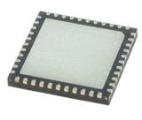
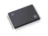
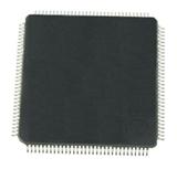
LFXP2-8E-5TN144I
FPGA - 现场可编程门阵列 8K LUTs 100 I/O Inst on DSP 1.2V -5 Spd
Architecture Overview LFXP2-8E-5TN144I
Each LatticeXP2 device contains an array of logic blocks surrounded by Programmable I/O Cells (PIC). Interspersed between the rows of logic blocks are rows of sysMEM™ Embedded Block RAM (EBR) and a row of sysDSP™ Digital Signal Processing blocks as shown in Figure 2-1.
Features LFXP2-8E-5TN144I
flexiFLASH™ Architecture
• Instant-on
• Infinitely reconfigurable
• Single chip
• FlashBAK™ technology
• Serial TAG memory
• Design security
Live Update Technology
• TransFR™ technology
• Secure updates with 128 bit AES encryption
• Dual-boot with external SPI
sysDSP™ Block
• Three to eight blocks for high performance
Multiply and Accumulate
• 12 to 32 18x18 multipliers
• Each block supports one 36x36 multiplier or four
18x18 or eight 9x9 multipliers
Embedded and Distributed Memory
• Up to 885 Kbits sysMEM™ EBR
• Up to 83 Kbits Distributed RAM
sysCLOCK™ PLLs
• Up to four analog PLLs per device
• Clock multiply, divide and phase shifting
Flexible I/O Buffer
• sysIO™ buffer supports:
– LVCMOS 33/25/18/15/12; LVTTL
– SSTL 33/25/18 class I, II
– HSTL15 class I; HSTL18 class I, II
– PCI
– LVDS, Bus-LVDS, MLVDS, LVPECL, RSDS
Pre-engineered Source Synchronous
Interfaces LFXP2-8E-5TN144I
• DDR / DDR2 interfaces up to 200 MHz
• 7:1 LVDS interfaces support display applications
• XGMII


企业名:深圳市中立信电子科技有限公司
类型:贸易/代理/分销
电话:
0755-23956688
0755-23956688
手机:13410226883
联系人:叶先生/王先生
QQ:
邮箱:Lee@zlxele.com
地址:广东深圳深圳市福田区彩田路彩虹新都大厦彩荟阁7A室