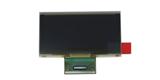


HGS25664A
清达光电
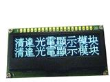
3.12寸
SSD1322
企业名:杭州清达光电技术有限公司
类型:原厂制造商
电话: 13506715842
手机:13506715842
联系人:卢小姐
QQ: 
微信:
邮箱:752574498@qq.com
地址:浙江杭州杭州市余杭区仁和街道永泰路2号22幢
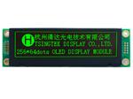
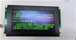
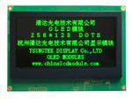
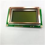
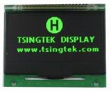
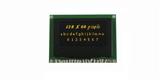
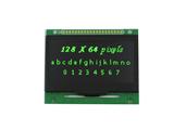
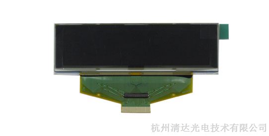
电子标签上用25664OLED显示屏,该屏为长条形256*64分辨率的OLED显示屏,尺寸为3.12寸,内置SSD1322控制器,电压5/3v可选,接口为8080并口/SPI串口/I2C串口,显示效果为黑底黄字/黑底绿字/黑底白字
HGS25664A介绍如下
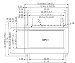
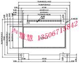
1) Outline Drawing: According to the annexed outline drawing
2) Number of Pixels: 256 × 64
3) Panel Size: 88.00 × 27.80 × 2.00 (mm)
4) Active Area: 76.78 × 19.18 (mm)
5) Pixel Pitch: 0.30 × 0.30 (mm)
6) Pixel Size: 0.28 × 0.28 (mm)
7) Weight: 9.95 (g)
电子标签上用25664OLED显示屏
1.5 Pin Definition
Pin Number Symbol Type Function
Power Supply
26 VCI P
Power Supply for Operation
This is a voltage supply pin. It must be connected to
external source & always be equal to or higher than VDD
& VDDIO.
25 VDD P
Power Supply for Core Logic Circuit
This is a voltage supply pin. It can be supplied
externally (within the range of 2.4~2.6V) or regulated
internally from VCI. A capacitor should be connected
between this pin & VSS under all circumstances.
24 VDDIO P
Power Supply for I/O Pin
This pin is a power supply pin of I/O buffer. It should
be connected to VDD or external source. All I/O signal
should have VIH reference to VDDIO. When I/O signal
pins (BS0~BS1, D0~D7, control signals…) pull high,
they should be connected to VDDIO.
2 VSS P
Ground of Logic Circuit
This is a ground pin. It also acts as a reference for the
logic pins. It must be connected to external ground.
3, 29 VCC P
Power Supply for OEL Panel
These are the most positive voltage supply pin of the
chip. They must be connected to external source.
5, 28 VLSS P
Ground of Analog Circuit
These are the analog ground pins. They should be
connected to VSS externally.
Driver
22 IREF I
Current Reference for Brightness Adjustment
This pin is segment current reference pin. A resistor
should be connected between this pin and VSS. Set the
current lower than 10uA.
4 VCOMH P
Voltage Output High Level for COM Signal
This pin is the input pin for the voltage output high level
for COM signals. A tantalum capacitor should be
connected between this pin and VSS.
27 VSL P
Voltage Output Low Level for SEG Signal
This is segment voltage reference pin.
When external VSL is not used, this pin should be left
open.
When external VSL is used, this pin should connect with
resistor and diode to ground.
Testing Pads
21 FR O
Cascade Application Connection Pin
This pin is No Connection pins. Nothing should be
connected to this pin. It should be left open individually.
1.5 Pin Definition (Continued)
Pin Number Symbol I/O Function
Interface
16
17
BS0
BS1 I
Communicating Protocol Select
These pins are MCU interface selection input. See the
following table:
BS0 BS1
3-wire SPI 1 0
4-wire SPI 0 0
8-bit 68XX Parallel 1 1
8-bit 80XX Parallel 0 1
20 RES# I
Power Reset for Controller and Driver
This pin is reset signal input. When the pin is low,
initialization of the chip is executed.
19 CS# I
Chip Select
This pin is the chip select input. The chip is enabled for
MCU communication only when CS# is pulled low.
18 D/C# I
Data/Command Control
This pin is Data/Command control pin. When the pin is
pulled high, the input at D7~D0 is treated as display data.
When the pin is pulled low, the input at D7~D0 will be
transferred to the command register. For detail
relationship to MCU interface signals, please refer to the
Timing Characteristics Diagrams.
14 E/RD# I
Read/Write Enable or Read
This pin is MCU interface input. When interfacing to a
68XX-series microprocessor, this pin will be used as the
Enable (E) signal. Read/write operation is initiated when
this pin is pulled high and the CS# is pulled low.
When connecting to an 80XX-microprocessor, this pin
receives the Read (RD#) signal. Data read operation is
initiated when this pin is pulled low and CS# is pulled
low.
When serial mode is selected, this pin must be connected
to VSS.
15 R/W# I
Read/Write Select or Write
This pin is MCU interface input. When interfacing to a
68XX-series microprocessor, this pin will be used as
Read/Write (R/W#) selection input. Pull this pin to
“High” for read mode and pull it to “Low” for write
mode.
When 80XX interface mode is selected, this pin will be
the Write (WR#) input. Data write operation is initiated
when this pin is pulled low and the CS# is pulled low.
When serial mode is selected, this pin must be connected
to VSS.
6~13 D7~D0 I/O
Host Data Input/Output Bus
These pins are 8-bit bi-directional data bus to be
connected to the microprocessor’s data bus. When serial
mode is selected, D1 will be the serial data input SDIN
and D0 will be the serial clock input SCLK.
Unused pins must be connected to VSS except for D2 in
serial mode.
1.5 Pin Definition (Continued)
Pin Number Symbol I/O Function
Reserve
23 N.C. -
Reserved Pin
The N.C. pin between function pins are reserved for
compatible and flexible design.
1, 30 N.C. (GND) -
Reserved Pin (Supporting Pin)
The supporting pins can reduce the influences from
stresses on the function pins. These pins must be
connected to external ground.
企业名:杭州清达光电技术有限公司
类型:原厂制造商
电话: 13506715842
手机:13506715842
联系人:卢小姐
QQ:
微信:
邮箱:752574498@qq.com
地址:浙江杭州杭州市余杭区仁和街道永泰路2号22幢