
企业名:深圳市云迪科技有限公司
类型:贸易/代理/分销
电话:
0755-23038182
0755-21015360
手机:15219483667
15919480276
联系人:朱先生/程小姐
QQ: 
邮箱:470889913@qq.com
地址:广东深圳深圳市福田区振兴路华康大厦1栋430
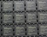
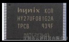
The Hynix HY27UF(08/16)1G2A series is a 128Mx8bit with spare 4Mx8 bit capacity. The device is offered in 3.3V Vcc Power Supply. Its NAND cell provides the most cost-effective solution for the solid state mass storage market. The memory is divided into blocks that can be erased independently so it is possible to preserve valid data while old data is erased. The device contains 1024 blocks, composed by 64 pages consisting in two NAND structures of 32 series connected Flash cells. A program operation allows to write the 2112-byte page in typical 200us and an erase operation can be performed in typical 2ms on a 128K-byte(X8 device) block. Data in the page can be read out at 30ns cycle time per byte. The I/O pins serve as the ports for address and data input/output as well as command input. This interface allows a reduced pin count and easy migration towards different densities, without any rearrangement of footprint. Commands, Data and Addresses are synchronously introduced using CE, WE, ALE and CLE input pin. The on-chip Program/Erase Controller automates all program and erase functions including pulse repetition, where required, and internal verification and margining of data. The modify operations can be locked using the WP input pin or using the extended lock block feature described later. The output pin R/B (open drain buffer) signals the status of the device during each operation. In a system with multiple memories the R/B pins can be connected all together to provide a global status signal. Even the write-intensive systems can take advantage of the HY27UF(08/16)1G2A extended reliability of 100K program/erase cycles by providing ECC (Error Correcting Code) with real time mapping-out algorithm. The chip could be offered with the CE don’t care function. This function allows the direct download of the code from the NAND Flash memory device by a microcontroller, since the CE transitions do not stop the read operation. The copy back function allows the optimization of defective blocks management: when a page program operation fails the data can be directly programmed in another page inside the same array section without the time consuming serial data insertion phase. The cache program feature allows the data insertion in the cache register while the data register is copied into the flash array. This pipelined program operation improves the program throughput when long files are written inside the memory. A cache read feature is also implemented. This feature allows to dramatically improve the read throughput when consecutive pages have to be streamed out. The HYNIX HY27UF(08/16)1G2A series is available in 48 - TSOP1 12 x 20 mm, 48 - USOP 12 x 17 mmm, FBGA 9 x 11 mm.
企业名:深圳市云迪科技有限公司
类型:贸易/代理/分销
电话:
0755-23038182
0755-21015360
手机:15219483667
15919480276
联系人:朱先生/程小姐
QQ:
邮箱:470889913@qq.com
地址:广东深圳深圳市福田区振兴路华康大厦1栋430
友情链接: 深圳市元东发电子有限公司