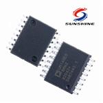


W9825G6KH-6
WINBOND
TSOP54
17+
企业名:深圳市尚想信息技术有限公司
类型:贸易/代理/分销
电话:
0755-83948880
0755-8398880
手机:15323892334
18182115682
联系人:姚小姐/邓小姐
QQ: 
微信:
邮箱:assistant@sunshineic.com
地址:广东深圳福田区振兴路上步工业区405栋6楼603室
7.1 Power Up and Initialization The default power up state of the mode register is unspecified. The following power up and initialization sequence need to be followed to guarantee the device being preconditioned to each user specific needs. During power up, all VDD and VDDQ pins must be ramp up simultaneously to the specified voltage when the input signals are held in the “NOP” state. The power up voltage must not exceed VDD + 0.3V on any of the input pins or VDD supplies. After power up, an initial pause of 200 μS is required followed by a precharge of all banks using the precharge command. To prevent data contention on the DQ bus during power up, it is required that the DQM and CKE pins be held high during the initial pause period. Once all banks have been precharged, the Mode Register Set Command must be issued to initialize the Mode Register. An additional eight Auto Refresh cycles (CBR) are also required before or after programming the Mode Register to ensure proper subsequent operation. 7.2 Programming Mode Register After initial power up, the Mode Register Set Command must be issued for proper device operation. All banks must be in a precharged state and CKE must be high at least one cycle before the Mode Register Set Command can be issued. The Mode Register Set Command is activated by the low signals of RAS , CAS, CS and WE at the positive edge of the clock. The address input data during this cycle defines the parameters to be set as shown in the Mode Register Operation table. A new command may be issued following the mode register set command once a delay equal to tRSC has elapsed. Please refer to the next page for Mode Register Set Cycle and Operation Table
企业名:深圳市尚想信息技术有限公司
类型:贸易/代理/分销
电话:
0755-83948880
0755-8398880
手机:15323892334
18182115682
联系人:姚小姐/邓小姐
QQ:
微信:
邮箱:assistant@sunshineic.com
地址:广东深圳福田区振兴路上步工业区405栋6楼603室