是
氧化铝陶瓷
*缘装置陶瓷
单晶
多种(mm)
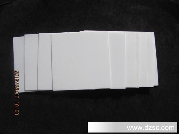
22*28*1,20*26*1,24*18.5*0.63
24*18.5*0.63,21*37*0.63,26*48*0.63
98*21*0.63,72*72*0.63,115*115*0.63
类型:生产企业
电话: 86 755 29825631
联系人:何龙飞
地址:广东深圳中国 广东 深圳市宝安区 沙井镇步涌村大园根二路8号
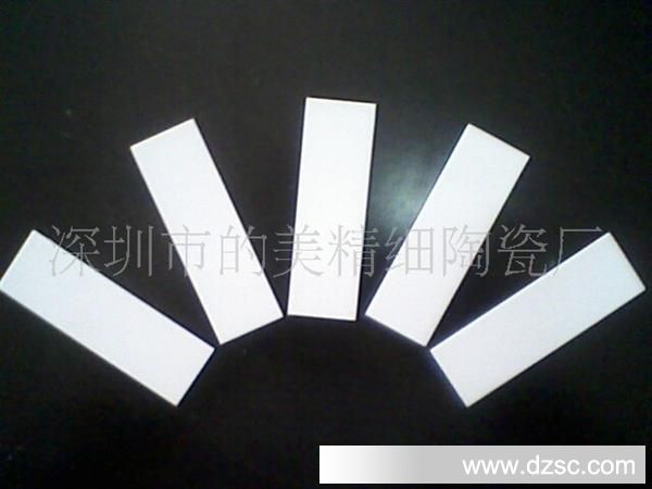


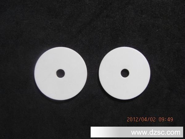


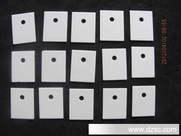
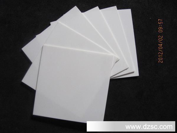
陶瓷基片,又称陶瓷基板,是以电子陶瓷为基底,对膜电路元件及外贴切元件形成一个支撑底座的片状材料。
按照陶瓷基片应用领域的不同,又分为HIC(混合集成电路)陶瓷基片、聚焦电位器陶瓷基片、激光加热定影陶瓷基片、片式电阻基片、网络电阻基片等;按加工方式的不同,陶瓷基片分为模压片、激光划线片两大类。
模压片
主要特点
陶瓷基片具有*、电*缘性能高、介电常数和介质损耗低、热导率大、化学稳定性好、与元件的热膨胀系数相近等主要优点,但陶瓷基片较脆,制成的基片面积较小,成本高。
发展方向
随着微电子技术的进步,微加工工艺的特征线宽已达亚*,一块基板上可以集成106~109个以上元件,电路工作的速度越来越快、频率越来越高,这对基板材料的性能提出了更高的要求。作为混合集成电路(HIC)和多芯片组件(MCM)的关键材料之一,基板占其总成本的60%左右。陶瓷基板发展的总方向是低介电常数、高热导率和*化。
目前,实际生产和开发应用的陶瓷基片材料有Al2O3、AlN、SiC、BeO、BN、莫来石和玻璃陶瓷等。其中,BeO和SiC热导率很高(³250W/m.K),但BeO因具有毒性,应用范围小,故产量低;SiC因体积电阻较小(<1013W·cm)、介电常数较大(40)、介电损耗较高(50),不利于信号的传输,且成型工艺复杂、设备昂贵,故应用范围也很小;AlN陶瓷基片是新一代*陶瓷基片,具有很高的热导率(理论值为319W/m.K,商品化的AlN基片热导率大于140W/m.k)、较低的介电常数(8.8)和介电损耗(~4×104)、以及和硅相配比的热膨胀系数(4.4×10-4/℃)等优点,但由于成本居高,一直没能大规模应用;Al2O3陶瓷基片虽然热导率不高(20W/m.K),但因其生产工艺相对简单,成本较低,价格便宜,成为目前*广泛应用的陶瓷基片。
深圳市的美科技电子有限公司一般采用流延成型法制备氧化铝陶瓷基片,目前发展到使用非苯系、*、*溶剂体系,对环境无污染,且流延坯片的干燥速率易于控制,配料中使用的溶剂可回收循环利用。在流延生坯上可以冲制各种形状和孔,然后进行烧成,可在连续式空气气氛窑炉中同时完成排胶和烧成的生产方式。96%氧化铝陶瓷基片材料中添加了合适的矿物原料作为助熔剂,烧成温度*1580℃~1600℃,产品密度即可达3.75g/cm3以上。对于尺寸精度要求较高的产品,可以在烧成后,以激光加工方法,在基片上划线、打孔,精度*&plu*n;0.05mm。
Ceramic substrate, also called ceramic substrates, electronic ceramic substrate is for, to film circuit components and the appropriate elements to form a support base, sheet material. According to the different of the application of ceramic substrate, and divided into HIC (hybrid integrated circuit) ceramic substrate, the focus potentiometer ceramic substrate, the laser heating fuser ceramic substrate, the chip resistor substrate, the network resistors substrate, etc.; According to the different methods of processing, ceramic substrate is divided into moulding piece, laser crossed piece two kinds big. Moulded piece of
The main features of high-temperature ceramic substrate, electric insulation performance is high, dielectric constant and medium loss, low thermal conductivity, good stability, and chemical components such as thermal expansion coefficient of similar major advantages, but brittle ceramic substrate, the area more ? made substrate
The main features
Ceramic substrate with high temperature, electric insulation performance is high, dielectric constant and medium loss, low thermal conductivity, good stability, and chemical components such as thermal expansion coefficient of similar major advantages, but brittle ceramic substrate, made of substrate area is lesser, high cost.
Development direction
Along with the progress of the microelectronics technology, the processing technology of the characteristic line width has reached a sub-micron, a piece of substrate can be integrated 106 ~ 109 more elements, circuit to work faster and faster, higher frequency, the substrate materials performance put forward higher request. As a hybrid integrated circuit cracking (HIC) and multichip module (MCM) one of the key materials, boards of its total cost of about 60%. Ceramic substrates development direction is always low dielectric often ?
The beauty of shenzhen science and technology electronic ceramics Co., LTD. General use of the flow ChengXingFa alumina ceramic substrate delay preparation, the present development to use the benzene department, non-toxic, pollution-free solvent systems, free from pollution to the environment, and the flow of billet delay the drying rate of easy to control, ingredients used in solvent recovery recycling. In the flow can be blunt the green delay of various shapes and hole, then firing, can be in the continuous air atmosphere in kiln finish at the same time row glue and firing mode of production. 96% alumina ceramic substrate materials added to the mineral right as raw material flux, firing temperature to 1580℃~ 1600 low℃, the product can reach 3.75 g density/cm3 above. For size higher accuracy of products, can be in
友情链接: 深圳市元东发电子有限公司