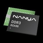
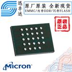

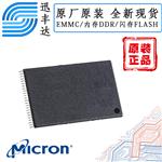
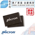
MT47H32M16NF-25E IT:H
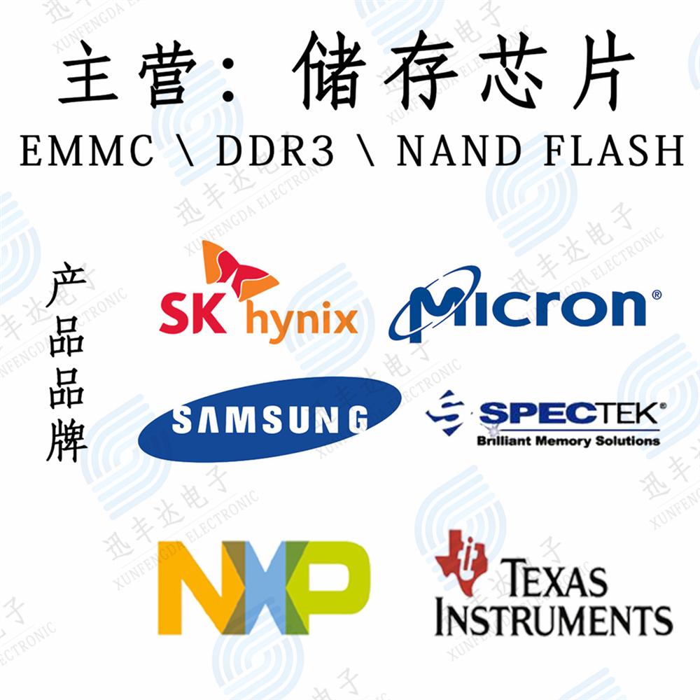
MICRON/镁光
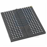
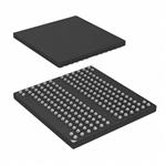
FBGA
21+/22+
84
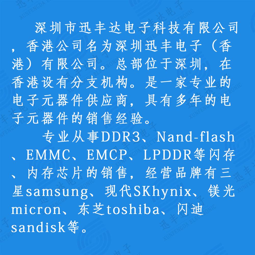
企业名:深圳市迅丰达电子科技有限公司
类型:贸易/代理/分销
电话: 13824331138
手机:13824331138
联系人:陈小姐
QQ: 
微信:
邮箱:491961368@qq.com
地址:广东深圳赛格广场3504A
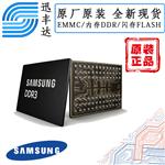
原装 MT47H32M16NF-25E IT:H DDR2
动态随机存取存储器 DDR2 512M 32MX16 FBGA
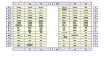
SDRAM - DDR2 存储器 IC 512Mb(32M x 16) 并联 400 MHz 400 ps 84-FBGA(8x12.5)
原装 MT47H32M16NF-25E IT:H DDR2 的技术参数:
制造商 : Micron Technology Inc.
存储器类型 : 易失
存储器格式 : DRAM
技术 : SDRAM - DDR2
存储容量 : 512Mb(32M x 16)
存储器接口 : 并联
时钟频率 : 400 MHz
写周期时间 - 字,页 : 15ns
访问时间 : 400 ps
电压 - 供电 : 1.7V ~ 1.9V
工作温度 : -40°C ~ 85°C(TA)
安装类型 : 表面贴装型
封装/外壳 : 84-TFBGA
供应商器件封装 : 84-FBGA(8x12.5)
基本产品编号 : MT47H32M16
RoHS 状态 : 符合 ROHS3 规范
湿气敏感性等级 (MSL) : 3(168 小时)
REACH 状态 : 非 REACH 产品
ECCN : EAR99
HTSUS : 8542.32.0028
原装 MT47H32M16NF-25E IT:H DDR2 的描述:
The DDR2 SDRAM uses a double data rate architecture to achieve high-speed operation. The double data rate architecture is essentially a 4n-prefetch architecture, with an interface designed to transfer two data words per clock cycle at the I/O balls.
A single READ or WRITE operation for the DDR2 SDRAM effectively consists of a single 4n-bitwide, two-clock-cycle data transfer at the internal DRAM core and four corresponding n-bit-wide, one-half-clock-cycle data transfers at the I/O balls.
A bidirectional data strobe (DQS, DQS#) is transmitted externally, along with data, for use in data capture at the receiver. DQS is a strobe transmitted by the DDR2 SDRAM during READs and by the memory controller during WRITEs.
DQS is edge-aligned with data for READs and center-aligned with data for WRITEs. The x16 offering has two data strobes, one for the lower byte (LDQS, LDQS#) and one for the upper byte (UDQS,UDQS#).
The DDR2 SDRAM operates from a differential clock (CK and CK#); the crossing of CK going HIGH and CK# going LOW will be referred to as the positive edge of CK. Commands (address and control signals) are registered at every positive edge of CK.
Input data is registered on both edges of DQS, and output data is referenced to both edges of
DQS as well as to both edges of CK.
Read and write accesses to the DDR2 SDRAM are burst-oriented; accesses start at a selected location and continue for a programmed number of locations in a programmed
sequence. Accesses begin with the registration of an ACTIVATE command, which is then
followed by a READ or WRITE command. The address bits registered coincident with
the ACTIVATE command are used to select the bank and row to be accessed. The address bits registered coincident with the READ or WRITE command are used to select
the bank and the starting column location for the burst access.
The DDR2 SDRAM provides for programmable read or write burst lengths of four or
eight locations. DDR2 SDRAM supports interrupting a burst read of eight with another
read or a burst write of eight with another write. An auto precharge function may be enabled to provide a self-timed row precharge that is initiated at the end of the burst access.
As with standard DDR SDRAM, the pipelined, multibank architecture of DDR2 SDRAM
enables concurrent operation, thereby providing high, effective bandwidth by hiding
row precharge and activation time.
A self refresh mode is provided, along with a power-saving, power-down mode.
All inputs are compatible with the JEDEC standard for SSTL_18. All full drive-strength
outputs are SSTL_18-compatible

企业名:深圳市迅丰达电子科技有限公司
类型:贸易/代理/分销
电话: 13824331138
手机:13824331138
联系人:陈小姐
QQ:
微信:
邮箱:491961368@qq.com
地址:广东深圳赛格广场3504A