深圳市宏德伟创科技有限公司(美国泰德授权代理)
(原厂原装,美国设计,原厂技术支持,质量保证)
联系人:张小姐 电话:0755-82812982 传真:0755-82812982
QQ:1027977946

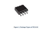
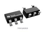
The TD1410 is a 380 KHz fixed frequency monolithic
step down switch mode regulator with a built in internal
Power MOSFET. It achieves 2A continuous output
current over a wide input supply range with excellent
load and line regulation.
The device includes a voltage reference, oscillation
circuit, error amplifier, internal PMOS and etc.
The PWM control circuit is able to adjust the duty ratio
linearly from 0 to 100%. An enable function, an over
current protection function and a short circuit protection
function are built inside. An internal compensation block
is built in to minimize external component count.
The TD1410 serves as ideal power supply units for
portable devices.
Applications
z Portable DVD
z LCD Monitor / TV
z Battery Charger
z ADSL Modem
z Telecom / Networking Equipment
The maximum junction temperature of TD1410 is 145°C,
which limits the maximum load current capability. Please
see the thermal de-rating curves for the maximum load
current of the TD1410 under different ambient
temperatures.
The thermal performance of the TD1410 is trongly
affected by the PCB layout. Extra care should be taken
by users during the design process to nsure that the IC
will operate under the recommended environmental
conditions.
Several layout tips are listed below for the best electric
and thermal performance.
1. Do not use thermal relief connection to the VIN and
the GND pin. Pour a maximized copper area to the GND
pin and the VIN pin to help thermal dissipation.
2. Input capacitor should be connected to the VIN pin
and the GND pin as close as possible.
3. Make the current trace from VOUT pins to L to the
GND as short as possible.
4. Pour copper plane on all unused board area and
connect it to stable DC nodes, like VIN, GND, or VOUT.
5. Keep sensitive signal traces such as trace connecting
FB pin away from the VOUT pins.
泰德授权全系列产品,可看代理证,可含税,欢迎联系咨询!