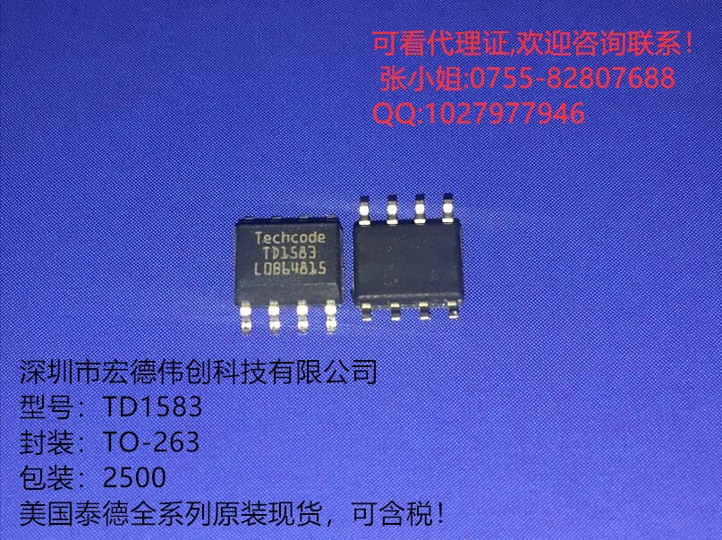
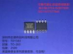
深圳市宏德伟创科技有限公司(美国泰德授权代理可看证)
(原厂原装,美国设计,原厂技术支持,质量保证)
联系人:张小姐 QQ:1027977946
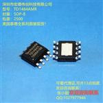
泰德TD1583性能概要:
(1)非常低压差操作:100%占空比
(2)宽的输入电压范围3.6V至28V
(3)宽的输出电压范围1.22V至26V
(4)输出电流3A
(5)固定开关频率:380KHz
(6)高效率:达93%
(7)过流保护,过热关断保护
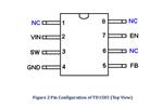
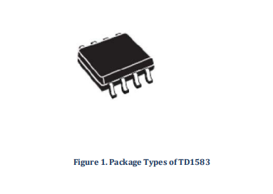
(8)SOP-8封装
应用领域:
便携式DVD
液晶显示器/电视
电池充电器
ADSL调制解调器
电信/网络设备等等
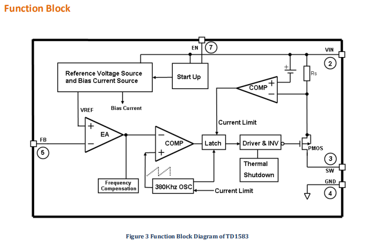
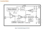
The TD1583 is a 380 KHz fixed frequency monolithic
step down switch mode regulator with a built in internal
Power MOSFET. It achieves 3A continuous output
current over a wide input supply range with excellent
load and line regulation.
The device includes a voltage reference, oscillation
circuit, error amplifier, internal PMOS and etc.
The PWM control circuit is able to adjust the duty ratio
linearly from 0 to 100%. An enable function, an over
current protection function and a short circuit protection
function are built inside. An internal compensation block
is built in to minimize external component count.
The TD1583 serves as ideal power supply units for
portable devices.
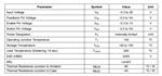
The maximum junction temperature of TD1583 is 145°C,
which limits the maximum load current capability. Please
see the thermal de-rating curves for the maximum load
current of the TD1583 under different ambient
temperatures.
The thermal performance of the TD1583 is trongly
affected by the PCB layout. Extra care should be taken
by users during the design process to nsure that the IC
will operate under the recommended environmental
conditions.
Several layout tips are listed below for the best electric
and thermal performance.
1. Do not use thermal relief connection to the VIN and
the GND pin. Pour a maximized copper area to the GND
pin and the VIN pin to help thermal dissipation.
2. Input capacitor should be connected to the VIN pin
and the GND pin as close as possible.
3. Make the current trace from VOUT pins to L to the
GND as short as possible.
4. Pour copper plane on all unused board area and
connect it to stable DC nodes, like VIN, GND, or VOUT.
5. Keep sensitive signal traces such as trace connecting
FB pin away from the VOUT pins.
DC/DC降压系列。。。