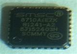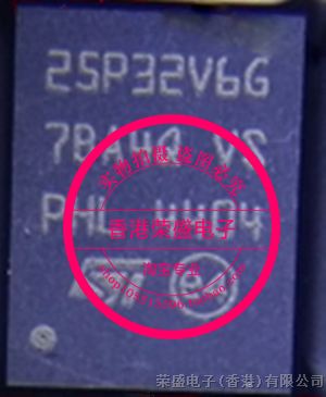
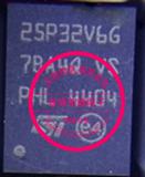
M25P32-VME6TG
ST
QFN-8
50MHz低压闪存
企业名:荣盛电子(香港)有限公司
类型:贸易/代理/分销
电话: 0755-82819399
手机:13530050576
联系人:蔡小姐
QQ: 
邮箱:hkrongsheng@163.com
地址:广东深圳门市:新亚洲电子市场一期4C005 公司:福田区中航路鼎城2203
M25P32-VME6TG
32 Mbit, Low Voltage, Serial Flash Memory
With 50MHz SPI Bus Interface

FEATURES SUMMARY
■ 32Mbit of Flash Memory
■ Page Program (up to 256 Bytes) in 1.4ms (typical)
■ Sector Erase (512Kbit)
■ Bulk Erase (32Mbit)
■ 2.7 to 3.6V Single Supply Voltage
■ SPI Bus Compatible Serial Interface
■ 50MHz Clock Rate (maximum)
■ Deep Power-down Mode 1μA (typical)
■ Electronic Signatures
– JEDEC Standard Two-Byte Signature (2016h)
– RES Instruction, One-Byte, Signature (15h), for backward compatibility
■ More than 100,000 Erase/Program Cycles per Sector
■ More than 20 Year Data Retention
SUMMARY DESCRIPTION
The M25P32 is a 32Mbit (4M x 8) Serial Flash Memory, with advanced write protection mechanisms,
accessed by a high speed SPI-compatible bus.
The memory can be programmed 1 to 256 bytes at a time, using the Page Program instruction.
The memory is organized as 64 sectors, each containing 256 pages. Each page is 256 bytes wide.
Thus, the whole memory can be viewed as consisting of 16384 pages, or 4,194,304 bytes.
The whole memory can be erased using the Bulk Erase instruction, or a sector at a time, using the
Sector Erase instruction.
SIGNAL DESCRIPTION
Serial Data Output (Q). This output signal is used to transfer data serially out of the device.
Data is shifted out on the falling edge of Serial Clock (C). Serial Data Input (D). This input signal
is used to transfer data serially into the device. It receives instructions, addresses, and the data to
be programmed. Values are latched on the rising edge of Serial Clock (C). Serial Clock (C). This
input signal provides the timing of the serial interface. Instructions, addresses, or data present
at Serial Data Input (D) are latched on the rising edge of Serial Clock (C). Data on Serial Data Output (Q)
changes after the falling edge of Serial Clock (C). Chip Select (S). When this input signal is High,
the device is deselected and Serial Data Output (Q) is at high impedance. Unless an internal Program,
Erase or Write Status Register cycle is in progress, the device will be in the Standby Power
mode (this is not the Deep Power-down mode). Driving Chip Select (S) Low enables the device,
placing it in the Active Power mode. After Power-up, a falling edge on Chip Select (S)
is required prior to the start of any instruction. Hold (HOLD). The Hold (HOLD) signal is used to
pause any serial communications with the device without deselecting the device.
During the Hold condition, the Serial Data Output (Q) is high impedance, and Serial Data Input (D)
and Serial Clock (C) are Don’t Care. To start the Hold condition, the device must be selected,
with Chip Select (S) driven Low. Write Protect (W). The main purpose of this input
signal is to freeze the size of the area of memory that is protected against program or erase
instructions (as specified by the values in the BP2, BP1 and BP0 bits of the Status Register).
企业名:荣盛电子(香港)有限公司
类型:贸易/代理/分销
电话: 0755-82819399
手机:13530050576
联系人:蔡小姐
QQ:
邮箱:hkrongsheng@163.com
地址:广东深圳门市:新亚洲电子市场一期4C005 公司:福田区中航路鼎城2203
友情链接: 深圳市元东发电子有限公司