FAIRCHILD/*童
FDN338P
结型(JFET)
P沟道
增强型
A/宽频带放大
SMD(SO)/表面封装
P-FET硅P沟道
3(V)
2(V)
1(μS)
0.5(pF)
类型:经销商
电话:
联系人:张新旭
地址:广东东莞中国 广东 东莞市 长安镇明和电子广场科技楼区F1702
∟ 结型场效应管(4)
FDN338P P-Channel Logic Level Enhancement Mode Field Effect Transistor
General Description
SuperSOT -3 P-Channel logic level enhancement mode power field effect transistors are produced using Fairchild's proprietary, high cell density, DMOS technology. This very high density process is especially tailored to minimize on-state resistance. These devices are particularly suited for low voltage applications in notebook computers, portable phones, PCMCIA cards, and other battery powered circuits where fast switching, and low in-line power loss are needed in a very *all outline surface mount package.
TM
Features
-1.6 A, -20 V, RDS(ON) = 0.13 @ VGS = -4.5 V RDS(ON) = 0.18 @ VGS = -2.5 V. Industry standard outline SOT-23 surface mount package using proprietary SuperSOTTM-3 design for *ior thermal and electrical capabilities. High density cell design for extremely low RDS(ON). Exceptional on-resistance and maximum DC current capability.
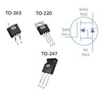
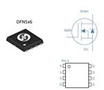
SuperSOTTM-3
SuperSOTTM-6
SuperSOTTM-8
SO-8
SOT-223
SOIC-16
D
D
8 33
S
SuperSOT -3
TM
G
G
S
Absolute Maximum Ratings
Symbol VDSS VGSS ID PD TJ,TSTG RJA RJC Parameter Drain-Source Voltage
TA = 25oC unless other wise noted FDN338P -20 8 -1.6 -5
(Note 1a) (Note 1b)
Units V V A
Gate-Source Voltage - Continuous Drain/Output Current - Continuous - Pulsed Maximum Power Dissipation
0.5 0.46 -55 to 150
W
Operating and Storage Temperature Range
C
THERMAL CHARA*ERISTICS Thermal Resistance, Junction-to-Ambient Thermal Resistance, Junction-to-Case
(Note 1a) (Note 1)
250 75
C/W C/W
(c) 1998 Fairchild Semiconductor Corporation
FDN338P Rev.D
Electrical Characteristics (TA = 25 OC unless otherwise noted )
Symbol Parameter Conditions Min T* Max Units OFF CHARA*ERISTICS BVDSS Drain-Source Breakdown Voltage Breakdown Voltage Temp. Coefficient Zero Gate Voltage Drain Current VGS = 0 V, ID = -250 A ID = -250 A, Referenced to 25 oC VDS = -16 V, VGS = 0 V TJ = 55C IGSSF IGSSR VGS(th) Gate - Body Leakage, Forward Gate - Body Leakage, Reverse
(Note)
-20 -28 -1 -10 100 -100
V mV/ oC A A nA nA
BVDSS/TJ
IDSS
VGS = 8 V,VDS = 0 V VGS = -8 V, VDS = 0 V VDS = VGS, ID = -250 A ID = -250 A, Referenced to 25 oC VGS = -4.5 V, ID = -1.6 A TJ =125C VGS = -2.5 V, ID = -1.3 A -0.4 -0.6 2 0.115 0.16 0.155 -2.5 3
ON CHARA*ERISTICS
Gate Threshold Voltage Gate Threshold Voltage Temp. Coefficient Static Drain-Source On-Resistance
-1
V mV/ oC
VGS(th)/TJ
RDS(ON)
0.13 0.22 0.18
ID(ON) gFS Ciss Coss Crss tD(on) tr tD(off) tf Qg Qgs Qgd IS VSD
Note:
On-State Drain Current Forward Transconductance
VGS = -4.5 V, VDS = -5 V VDS = -5 V, ID = -1.6 A VDS = -10 V, VGS = 0 V, f = 1.0 MHz
A S
DYNAMIC CHARA*ERISTICS Input Capacitance Output Capacitance Reverse Transfer Capacitance
(Note)
pF pF pF
SWITCHING CHARA*ERISTICS Turn - On Delay Time Turn - On Rise Time Turn - Off Delay Time Turn - Off Fall Time Total Gate Charge Gate-Source Charge Gate-Drain Charge
VDD = -5 V, ID = -1 A, VGS = -4.5 V, RGEN = 6
6.
.5
ns ns ns ns nC nC nC
VDS = -5 V, ID = -1.6 A, VGS = -4.5 V
6 0.8 1.3
DRAIN-SOURCE DIODE CHARA*ERISTICS AND MAXIMUM RATINGS Maximum Continuous Drain-Source Diode Forward Current Drain-Source Diode Forward Voltage VGS = 0 V, IS = -0.42 A
(Note)
-0.42 -0.7 -1.2
A V
1. RJA is the sum of the junction-to-case and case-to-ambient thermal resistance where the case thermal reference is defined as the solder mounting surface of the drain pins. RJC is guaranteed by design while RCA is determined by the user's board design. T*ical RJA using the board layouts shown below on FR-4 PCB in a still air environment :
a. 250oC/W when mounted on 0.02 in2 pad of 2oz Cu.
a
b. 270oC/W when mounted on a 0.001 in2 pad of 2oz Cu.
Scale 1 : 1 on letter size paper 2. Pulse Test: Pulse Width < 300s, Duty Cycle < 2.0%.
FDN338P Rev.D
T*ical Electrical Characteristics
10 -I D , DRAIN-SOURCE CURRENT (A) 2
RDS(ON) , *RMALIZED
8
VGS = -4.5V -4.0 -3.5
-3.0 -2.5
DRAIN-SOURCE ON-R*ISTANCE
1.8 1.6 1.4 1.2 1 0.8
VGS = -2.0V
6
-2.5 -3.0 -3.5 -4.0 -4.5
-2.0
4
2
-1.5
0
0
1
2
3
4
5
0
2
4
6
8
10
-VDS , DRAIN-SOURCE VOLTAGE (V)
-I D , DRAIN CURRENT (A)
Figure 1. On-Region Characteristics.
Figure 2. On-Resistance Variation with Drain Current and Gate Voltage.
1.6 DRAIN-SOURCE ON-R*ISTANCE
0.5
I D = -1.6A
1.4
V GS = -4.5V
R DS(ON) ,ON-R*ISTANCE(OHM)
I D = -0.8A
0.4
RDS(ON) , *RMALIZED
1.2
0.3
TJ = 125C
0.2
1
0.8
0.1
25C
0.6 -50
-25
0
25
50
75
100
125
150
0 1 -V 2
GS
3
4
5
TJ , JUN*ION TEMPERATURE (C)
,GATE TO SOURCE VOLTAGE (V)
Figure 3. On-Resistance Variation with Temperature.
Figure 4. On-Resistance Variation with Gate-to-Source Voltage.
-I S , REVERSE DRAIN CURRENT (A)
10
10
VDS = -5V
-I D , DRAIN CURRENT (A) 8
TA = -55C
VGS = 0V
1
25C 125C
6
0.1
T = 125C J 25C -55C
4
0.01
2
0.001
0
0. -VGS , GATE TO SOURCE VOLTAGE (V)
0
0.2
0.4
0.6
0.8
1
1.2
1.4
-V SD , BODY DIODE FORWARD VOLTAGE (V)
Figure 5. Transfer Characteristics.
Figure 6 . Body Diode Forward Voltage Variation with Source Current and Temperature.
FDN338P Rev.D
T*ical Electrical Characteristics
5 -V GS , GATE-SOURCE VOLTAGE (V) 1000
I D = -1.6A
4
V DS= -5V -15V
CAPACITANCE (pF)
00 50
C iss
3
Coss
2
1 20 0.1
f = 1 MHz V GS = 0 V
0.2 0.5 1 2 5
C rss
0
0
2
4 Q g , GATE CHARGE (nC)
6
8
10
20
-VDS , DRAIN TO SOURCE VOLTAGE (V)
Figure 7. Gate Charge Characteristics.
Figure 8. Capacitance Characteristics.
10 5 -I D, DRAIN CURRENT (A) 2 1 0.5
RD S( ON ) LIM IT
50
1m 10 s ms
POWER (W)
40
10 0m s
SINGLE PULSE R JA =250 C/W TA = 25C
1s 10s
30
0.1 0.05
VGS = -4.5V SINGLE PULSE RJA =250C/W T A = 25C A
0.2 0.5 -V
DS
DC
20
10
0.01 0.1
1
2
5
10
20
40
0 0.0001
0.001
0.01
0.1
1
10
100 300
, DRAIN-SOURCE VOLTAGE (V)
SINGLE PULSE TIME (SEC)
Figure 9. Maximum Safe Operating Area.
Figure 10. Single Pulse Maximum Power Dissipation.
1
r(t), *RMALIZED EFFE*IVE TRANSIENT THERMAL R*ISTANCE
0.5 0.2 0.1 0.05 0.02 0.01 0.005 0.002
D = 0.5 0.2 0.1 0.05 0.02 0.01 Single Pulse P(pk)
R JA (t) = r(t) * RJA R JA = 250 C/W
t1
t2
TJ - TA = P * RJA (t) Duty Cycle, D = t1 /t2
0.001 0.0001
0.001
0.01
0.1 t1 , TIME (sec)
1
10
100
300
Figure 11. Transient Thermal Response Curve.
FDN338P Rev.D
友情链接: 深圳市元东发电子有限公司