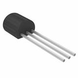


J112RLRAG
ON(安森美)
无铅环保型
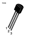
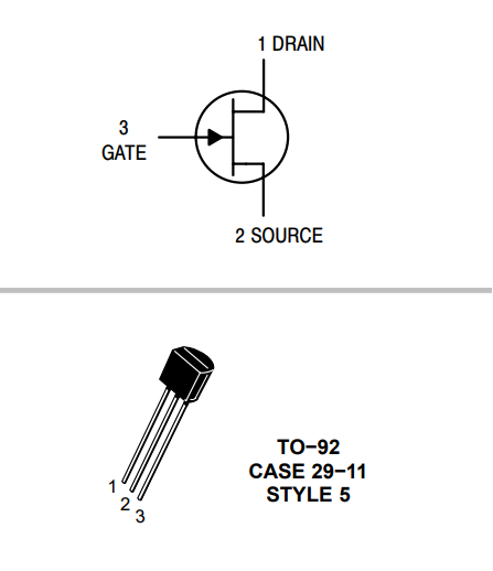
TO-92-3
35 V
5 mA
N-Channel
企业名:深圳市勤思达科技有限公司
类型:贸易/代理/分销
电话:
0755-83264115
0755-82710921
手机:15889758566
13714022780
联系人:朱亮成/18948336722
QQ: 
微信:
邮箱:1282971461@qq.com
地址:广东深圳深圳市福田区华强北赛格科技园四栋中12楼A4座—2L
型号:J112RLRAG J112RLRAG
品牌:ON
类别:分离式半导体产品
家庭:JFET(结点场效应
系列:-
电流 - 漏极(Idss) @ Vds (Vgs=0):5mA @ 15V
漏极至源极电压(Vdss):-
漏极电流 (Id) - :-
FET 型:N 沟道
电压 - 击穿 (V(BR)GSS):35V
电压 - 切断 (VGS 关)@ Id:1V @ 1μA
输入电容 (Ciss) @ Vds:-
电阻 - RDS(开):50 欧姆
安装类型:通孔
包装:带卷 (TR)
封装/外壳:TO-226-3、TO-92-3(TO-226AA)成形引线
供应商设备封装:TO-92-3
功率 - :350mW
其它名称:J112RLRAG-NDJ112RLRAGOSTR
标准包装:2000
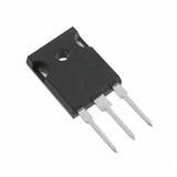
封装:TO-220
单价:面议
备注:额定值超出该设备损坏可能会发生这些值。施加到器件的额定值是个人压力限值(不正常工作条件下),并同时无效。如果这些限制超标,设备功能操作不暗示,可能会出现损伤和可靠性可能受到影响。
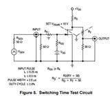
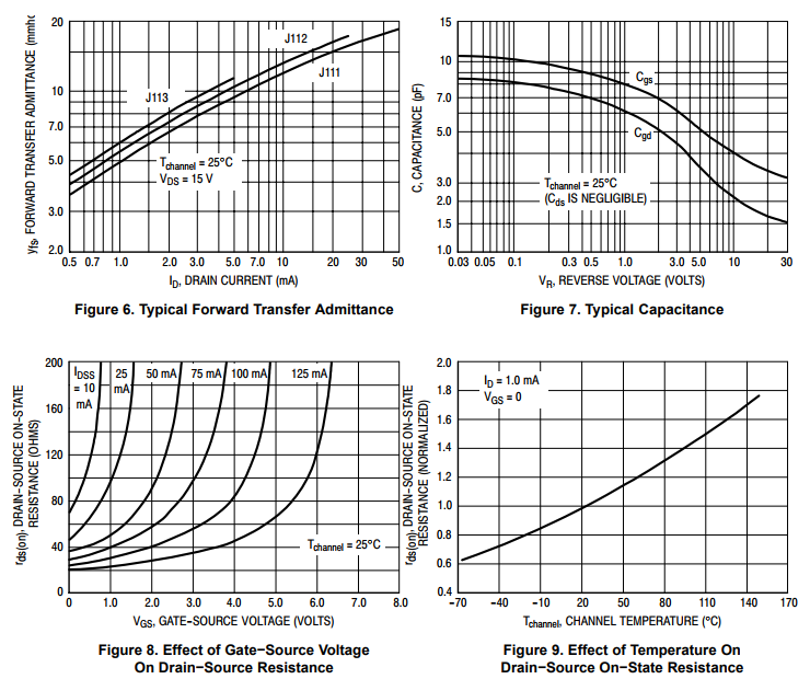
The switching characteristics shown above were measured using a test
circuit similar to Figure 5. At the beginning of the switching interval,
the gate voltage is at Gate Supply Voltage (−VGG). The Drain−Source
Voltage (VDS) is slightly lower than Drain Supply Voltage (VDD) due
to the voltage divider. Thus Reverse Transfer Capacitance (Crss) or
Gate−Drain Capacitance (Cgd) is charged to VGG + VDS.
During the turn−on interval, Gate−Source Capacitance (Cgs)
discharges through the series combination of RGen and RK. Cgd must
discharge to VDS(on) through RG and RK in series with the parallel
combination of effective load impedance (R′D) and Drain−Source
Resistance (rds). During the turn−off, this charge flow is reversed.
Predicting turn−on time is somewhat difficult as the channel resistance
rds is a function of the gate−source voltage. While Cgs discharges, VGS
approaches zero and rds decreases. Since Cgd discharges through rds,
turn−on time is non−linear. During turn−off, the situation is reversed
with rds increasing as Cgd charges.

企业名:深圳市勤思达科技有限公司
类型:贸易/代理/分销
电话:
0755-83264115
0755-82710921
手机:15889758566
13714022780
联系人:朱亮成/18948336722
QQ:
微信:
邮箱:1282971461@qq.com
地址:广东深圳深圳市福田区华强北赛格科技园四栋中12楼A4座—2L